Product Summary
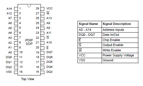
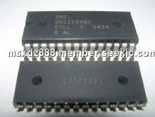
The U62256ADC-07LL is a standard 32K X 8 SRAM manufactured using a CMOS process technology with the following operating modes: Read - Standby, Write - Data Retention The U62256ADC-07LL memory array is based on a 6-transistor cell. The U62256ADC-07LL circuit is activated by the falling edge of E. The address and control inputs open simultaneously. According to the information of W and G, the data inputs, or outputs, are active. In a Read cycle, the U62256ADC-07LL data outputs are activated by the falling edge of G, afterwards the data word read will be available at the outputs DQ0-DQ7. After the address change, the data outputs go High-Z until the new information read is available. The data outputs have not preferred state.
Parametrics
U62256ADC-07LL absolute maximum ratings: (1) Power Supply Voltage VCC: -0.5, 7 V; (2) Input Voltage VI: -0.5 VCC, + 0.5 b V; (3) Output Voltage VO: -0.5 VCC, + 0.5 b V; (4) Power Dissipation PD: - 1 W; (5) Output Short Circuit Current at VCC = 5 V and VO = 0 V c | IOS |: 200 mA.
Features
U62256ADC-07LL features: (1) 32768x8 bit static CMOS RAM; (2) Access times 70 ns, 100 ns; (3) Common data inputs and data outputs; (4) Three-state outputs; (5) QS 9000 Quality Standard; (6) ESD protection > 2000 V (MIL STD 883C M3015.7); (7) Latch-up immunity >100 mA; (8) Packages: PDIP28 (600 mil) SOP28 (330 mil); (9) TTL/CMOS-compatible; (10) Automatical reduction of power dissipation in long Read Cycles.
Diagrams

 |
 U6220B |
 Other |
 |
 Data Sheet |
 Negotiable |
|
||||
 |
 U6223B |
 Other |
 |
 Data Sheet |
 Negotiable |
|
||||
 |
 U6223B-AFP |
 Other |
 |
 Data Sheet |
 Negotiable |
|
||||
 |
 U6224B |
 Other |
 |
 Data Sheet |
 Negotiable |
|
||||
 |
 U6224B-AFP |
 Other |
 |
 Data Sheet |
 Negotiable |
|
||||
 |
 U62256 |
 Other |
 |
 Data Sheet |
 Negotiable |
|
||||
 (China (Mainland))


